Food Food Why OEMs in Industry Are Struggling to Scale AI—and How a Centralized Platform Can Turn the Tide 20 May 2025 - Blog
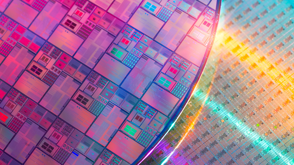
Semiconductor Semiconductor Wafer Map Defect Pattern Classification Methods, Challenges, and Opportunities 28 Mar 2025 - Blog
Semiconductor Semiconductor Wafer Defect Classification: Key Techniques and Industry Standards 24 Mar 2025 - Blog
Food Food Stop Guessing, Start Adapting: AI Retraining for Smarter Food Processing 14 Mar 2025 - Blog
Agriculture Agriculture AI in Agriculture: Sustainable Farming with Cutting-Edge Tech 07 Mar 2025 - Blog
Agriculture Agriculture 3D Vision and AI Robotics: The Future of Intelligent Automation 07 Mar 2025 - Blog