Wafer Map Defect Pattern Classification Methods, Challenges, and Opportunities
Date Section Blog

Wafer defect maps provide critical information about manufacturing defects. However, most images have no special spatial patterns and are full of noise, making wafer map defect pattern classification difficult. To overcome these challenges, several methods have been developed, providing a reliable and scalable way to detect defects during semiconductor manufacturing.
Using Wafer Maps to Identify Defect Root Cause
Worldwide, the demand for powerful semiconductor chips increases. As semiconductor manufacturing technology advances, the more complex and diverse wafer defects become in shape, size, and location. Because of this, manufacturers face new challenges in improving wafer defect detection accuracy. To identify errors quickly, they must better control individual processing steps—a difficult task when producing high chip volumes.
Wafer map defect pattern classification methods play a key role in overcoming this issue, offering important information about manufacturing defects. For example, a patterned defect can show which step in the process is incorrectly performed. If the same defect occurs multiple times, yield can rapidly decrease. But how exactly are wafer maps produced, and what methods and applications make them critical to identifying defects?
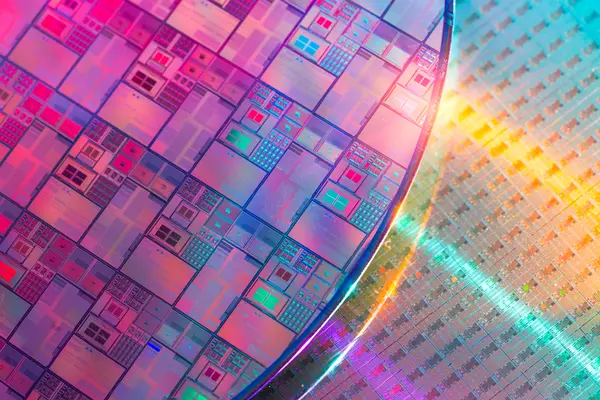
Wafer defect positions and types can be found at different stages of chip production. When displayed as an image, this is known as a wafer map. After wafer fabrication, each die in a wafer is tested to determine if the required functionality has been satisfied. The wafer's spatial information indicates which dies perform correctly and which fail. This information is represented in a two-dimensional array (a wafer map) produced by inspection machines that monitor and test the performance of individual circuits (ICs) on the wafer. The spatial pattern of passing and failing dies can indicate specific issues in the manufacturing process.
The Problem With Manual Inspection
Clustering wafer map images based on the types of observed defect patterns helps identify relevant defect patterns on wafer maps. These patterns offer insights for defect root-cause analysis. For example, a line on a wafer may indicate a device has scratched the wafer during a production step. However, the semiconductor manufacturing process is highly complex and variable. Recognizing scratch and line types of defect patterns is challenging for process and test engineers, and requires much manpower to identify such patterns. Particularly since hidden defective dies can exist on the scratch contour and become discontinuity points.
When large quantities of wafers are continuously produced, manual inspection is even less effective. New defects can occur constantly where labeled data is not available, and even for known defect patterns, labeling is time-intensive and requires expert knowledge. Building a classification model is a primary challenge, owing to the high cost of labeling wafer maps with defect categories to create a training dataset. While labeling single-defect wafer maps is easy thanks to their simple, clear patterns, labeling mixed-defect maps is difficult and time-consuming due to their often complex and ambiguous patterns.
Wafer Map Defect Pattern Classification Using Convolutional Neural Network
In recent years, considerable research has used machine learning to automate wafer map defect pattern classification. Studies use a convolutional neural network (CNN) as a classification model to process wafer maps directly with no manual feature extraction needed. Not only can a CNN can be trained to accurately classify mixed-defect maps with unlimited defect categories and no imposed assumptions on the test dataset; its predictive performance also improves with no extra data collection or labeling costs. The result is superior performance in wafer map pattern classification—and a method applicable to any CNN, with no architecture or learning objective restrictions.
Removing Noise From Input Data
Although CNNs provide effective wafer map classification, they have a major limitation: noise in the data. Wafer maps often contain noisy artifacts, such as random defects. These defects can mislead the CNN model toward inaccurate classification. To remove input data noise, Denoising Convolutional Neural Networks (DCNNs) allow the network to focus on relevant and informative features. Autoencoders, generative models, and denoising filters can also be used in image processing tasks where noise reduction boosts overall performance. These techniques offer advantages in denoising classic image problems such as grayscale or color images, text recovery, and image inpainting.
Autoencoder architectures can also preprocess wafer map images by cleaning up noisy pixels before feeding them to a classification network. Noise-aware models can improve classification accuracy when working with noisy datasets by learning to distinguish useful patterns from irrelevant noise. However, insufficient training data presents a significant challenge. A lack of well-annotated datasets hampers model performance and restricts the development of related algorithms. The classification accuracy mainly depends on the data quality, with low-quality data leading to over-fitting or inaccurate classifiers being trained. Good data preprocessing techniques are essential for data mining to improve data quality and increase classifier accuracy and efficiency.
Paving the Way for Reliable, Scaleable Defect Detection
Combining the strengths of autoencoder-based data augmentation and deep CNNs outperforms traditional machine learning methods, achieving a classification accuracy of 98.56% and improved generalization capabilities. By combining this with data purity solutions, manufacturers can overcome the challenges posed by imbalanced datasets and noise, enabling the model to learn more robustly from a broader and more diverse set of samples. These methods hold promise for effective wafer defect map pattern classification, providing a reliable and scalable tool for anomaly detection in semiconductor manufacturing.