Visual AI Inspection for PCB Assembly Quality Control
Date Section Blog
Electronic devices are becoming more compact, increasing the complexity of printed circuit board (PCB) assembly. This challenge makes high-quality standards hard to maintain. Automating defect detection using visual AI inspection transforms quality control, reducing human error and enabling faster production. By leveraging this technology for PCB assembly, manufacturers improve efficiency and overall product quality in high-volume electronics production.
Key Challenges in PCB Assembly Inspection
PCBs contain a vast array of components including resistors, capacitors, and transistors. Each is positioned according to the circuit’s layout and characteristics, requiring precise placement for optimal functionality. Components vary in number, size, appearance, and assembly specifications. Assembly is intricate, even minor defects, such as misaligned components, poor solder joints, or micro-cracks lead to device failures. The complexity of assembly demands meticulous inspection to confirm component placement and alignment, matched with designated serial numbers. This scrutiny is paramount to guarantee the functionality of the PCB. Traditional inspection methods struggle to keep pace with modern PCB designs — necessitating more advanced solutions.
Limitations of Conventional PCB Inspection
Visual PCB inspection traditionally relies on manual methods. However, manual inspection is error-prone due to the intricate nature of PCBs featuring multiple parts and configurations. Subtle differences go unnoticed by the human eye, resulting in inaccurate or missed detections. Inherent limitations make it difficult to optimize manual inspection which is time-consuming and error-prone, especially in high-volume production.
Other conventional rule-based inspection systems often encounter errors. On top of this, they need manual reinspection to boost detection accuracy. Traditional Automated Optical Inspection (AOI) systems offer some automation but are limited by pre-programmed defect detection. These systems also lack adaptability to new defect types. As PCBs become smaller and more densely packed, traditional methods become inadequate, necessitating advanced solutions like visual AI inspection.
What Is Visual AI in PCB Assembly?
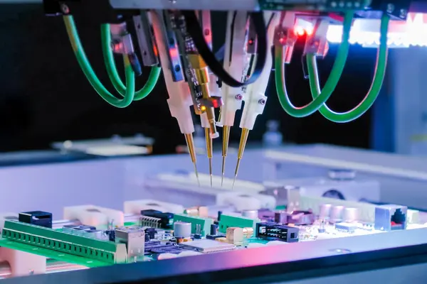
Visual AI inspection enables computers to interpret and analyze visual data. In electronics manufacturing, visual AI systems use high-resolution cameras and deep learning algorithms to capture and examine images of PCBs during assembly. Boards are continuously inspected as they move along the production line. Advanced algorithms analyze images to detect defects, and the system compares the inspected board to an image of a correctly assembled PCB. Any deviations affecting product performance are flagged for correction. By automating defect detection, Visual AI ensures that every board meets strict quality standards with minimal human intervention.
Optimizing PCB Quality Control with Visual AI Inspection
Component miniaturization creates increasingly complex inspection requirements. Modern Visual AI inspection systems meet this demand, enhancing efficiency and accuracy in electronics manufacturing. Equipped with high-resolution cameras and advanced image processing, these systems detect microscopic defects in high-definition detail. While AI algorithms detect multiple defect types simultaneously, including:
- Solder joint defects such as insufficient solder, bridging, and excess material
- Component placement errors like position misalignment and incorrect orientation
- Dimensional inconsistencies affecting circuit performance
Unlike traditional AOI, visual AI detects the newest and most challenging defects — such as micro-soldering issues — without frequent recalibration. The result is improved quality control, fewer product transition disruptions, and reduced rework and returns.
Key Benefits of Visual AI in PCB Assembly
AI-driven visual inspection eliminates inconsistencies inherent in manual and rule-based inspections. The likelihood of errors decreases due to the ability to detect defects too small for the human eye. And unlike human inspectors, AI does not experience fatigue, ensuring precision across all production runs. Other key benefits include:
Fast Inspection Speeds
AI-powered systems process thousands of images per minute. This speed helps increase production rates and accelerate time to market without compromising quality.
Lower Operational Costs
Automation reduces labor costs associated with manual inspections. Additionally, early detection of defects prevents defective boards progressing down the production line, minimizing rework and material waste.
Continuous Process Optimization
AI-based inspection tools provide continuous monitoring of PCB assembly lines, enabling immediate defect identification and correction. The collected data is analyzed to identify recurring defects and continuously refine production processes.
Higher Product Quality and Customer Satisfaction
With AI-driven solutions manufacturers reduce defects by maintaining strict quality standards. The result is fewer product returns, improved customer satisfaction, and protected brand reputation.
Applications of Visual AI in PCB Assembly Inspection
Visual AI technology has a crucial role in PCB assembly inspection. This advanced inspection method ensures precision and efficiency across various quality control processes. There are many visual AI PCB inspection examples, but below are three key applications:
- Automatic Optical Inspection (AOI): AOI is one of the most common vision AI applications in PCB manufacturing. These systems utilize high-resolution cameras and advanced algorithms to detect component misalignment, missing parts, and soldering defects. Inspections occur at various production stages, including pre-reflow (before soldering) and post-reflow (after soldering), ensuring defects are identified and addressed promptly.
- Solder Paste Inspection (SPI): During PCB assembly solder paste is applied to the board before component placement. Thickness or solder paste placement inconsistencies lead to poor solder joints and faulty products. AI vision-based SPI systems analyze solder paste application, ensuring specifications are met before component placement.
- 3D Imaging for Complex Defects: Visual AI inspection systems use 3D imaging to inspect PCBs with complex geometries. Some defects, such as component tilt or insufficient solder volume, may not be detectable in 2D images. The added dimension of AI-powered 3D imaging provides a more comprehensive view of PCBs, improving defect detection accuracy in complex assemblies.
Effective quality control in PCB assembly relies on advanced inspection techniques to detect defects early and ensure reliability. The use of visual AI technology across a wide range of applications is a key enabler in this process, helping to boost accuracy and maintain consistent production standards.
The Future of PCB Quality Control with Visual AI
Visual AI inspection is reshaping PCB quality assurance. By automating defect detection, manufacturers achieve unmatched precision, speed, and efficiency which leads to higher quality standards and shorter production timelines. As AI advances its role in electronics manufacturing expands, making it an essential tool for quality control. Investing in AI-driven visual inspection solutions is no longer optional — it is a strategic manufacturing imperative for staying competitive in an evolving industry.
Ready to learn about Robovision’s customizable vision AI platform for PCB defect detection? Head to our industry page for more information.