Top 5 Wafer Inspection Tools for Semiconductor Manufacturing
Date Section Blog
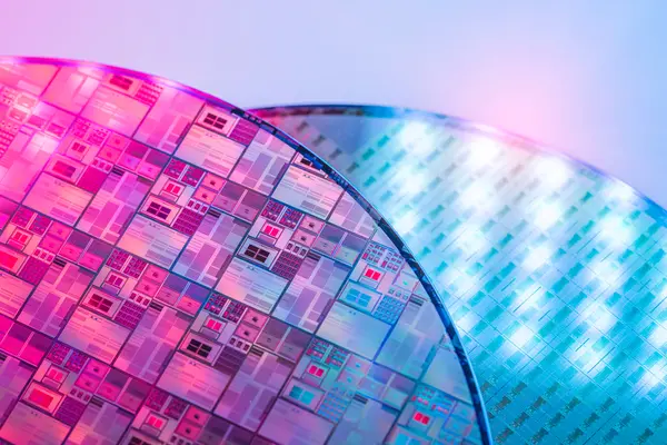
Semiconductor manufacturers rely on wafer inspection tools to detect microscopic defects that impact yield and performance. As process nodes shrink and chip complexity rises, advanced inspection systems ensure quality at every stage. This article explores five wafer inspection tools shaping the industry and improving defect detection rates in high-volume manufacturing.
Precision in Every Nanometer
Semiconductor manufacturing is advancing rapidly due to several key trends. The most significant is the push toward smaller nodes and more complex chip architectures to help improve performance, reduce power consumption, and increase efficiency. In recent years, microfabrication technology has reached the nanometer range. At the same time, expanding wafer diameters mean several thousand semiconductor chips with billions of transistors can now be produced from one single wafer. The industry is also approaching near-zero tolerances to known defect types such as particles and crystal defects. As progress continues into the nano-scale, device sensitivities to new types of defects are being discovered too. The result is increasing demand for metrology inspection tools to sense and quantify defects at near-noise level, together with the development of new advanced approaches to defect detection.
Wafer defect inspection tools are the gatekeepers of quality, ensuring each step in the complex fabrication process meets exacting standards. The latest advancements in metrology inspection and defect detection enable fabs to maintain production at scale, reducing costly scrap and rework while improving quality. The following five tools play a critical role in semiconductor wafer inspection, ensuring precision and reliability.
1. E-Beam Inspection
Electron beam (EB) inspection is essential for detecting nanoscale defects in leading-edge semiconductor nodes. Unlike optical methods, EB tools offer unparalleled resolution, capturing structural anomalies in advanced logic and memory devices. However, throughput remains a challenge. Slow measurement speeds make it more useful in R&D environments and new technology process development. Multi-beam EB systems address this limitation by scanning multiple areas simultaneously, balancing accuracy with efficiency. New tools are being developed with up to 100 columns, or channels of measurement.
2. Automated Defect Classification
Defect classification assigns an image of a defect to a specific category, ensuring fewer flaws go unnoticed and enabling predictive maintenance. A fully classified Pareto, listing yield-limiting defects by type, helps engineers quickly identify issues and trace root causes efficiently. Automatic Defect Classification (ADC) tools reduce reliance on human inspection but often struggle with accuracy in high-purity environments. Deep Learning AI-based classifiers improve accuracy, enabling precise classification of both known and emerging defect types across various wafer designs. Machine learning (ML) and AI are increasingly integrated into wafer inspection tools, providing fast, automated defect categorization. These advancements help engineers detect, monitor, and resolve critical yield excursions with greater efficiency. By enhancing defect classification speed and accuracy, AI-driven solutions improve quality control, ensuring higher yields in semiconductor manufacturing.
3. Dark-field Inspection
This method is preferred for inspecting large numbers of non-patterned wafers since high rastering speeds are possible. However, dark-field-based tools are also used to detect defects on patterned wafers with high sensitivity and throughput realized by sheet-beam optics and accurate light separation. The technique excels at identifying deviations in lithography, etch, and deposition processes, and provides a higher contrast signal for defects that conventional brightfield imaging might overlook. With semiconductor nodes reaching extreme ultraviolet (EUV) lithography levels, dark-field tools play a crucial role in quality control.
4. Differential Image Detection
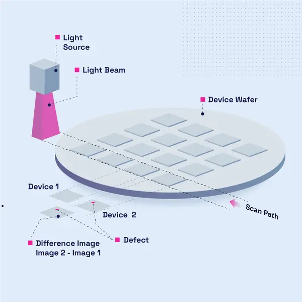
Patterned wafer optical inspection utilizes bright-field, dark-field, or a combination of both illumination methods for defect detection. These systems compare a test die’s image with that of an adjacent die or a known defect-free “golden” die. Image processing software subtracts one image from the other, highlighting any random anomalies that remain visible in the resulting image. Tools for differential image detection process enable the creation of defect maps, similar to those used in non-patterned wafer inspection. Precise, repeatable motion control of both the wafer stage and optical components is essential, as both must move simultaneously for accurate detection.
4.Deep Ultraviolet (DUV) Wafer Inspection
Defect inspection for sub-100 nm patterned wafers is more complex than non-patterned wafer inspection. DUV-based optical inspection, an industry standard for patterned wafers down to 65 nm, requires advanced optics, motion control, and image analysis. DUV inspection detects defects like shallow trench isolation voids and photoresist micro bridging, achieving the required sensitivity for dynamic random access memory (DRAM) and flash devices at 55 nm. While DUV systems offer high throughput and cost efficiency, they struggle with precision below 65 nm. Additionally, DUV laser illumination has caused issues like surface material ablation. To address these challenges, manufacturers are exploring broadband plasma illumination and production-capable electron beam inspection tools. Plasma-generated broadband illumination systems, now available for production environments, may provide the necessary sensitivity and accuracy for next-generation semiconductor fabrication.
5. Atomic Force Microscopy (AFM)
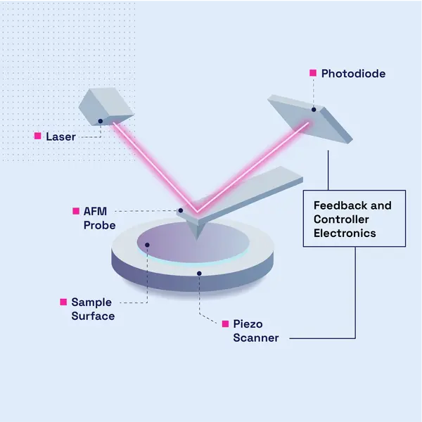
Precise feature dimensions on a wafer are critical to functionality and reliability. AFM tools provide atomic-level resolution for surface measurements with dimensions beyond the highest-resolution optical microscopes. Their main use is for detecting topographical variations and nanometer-scale defects in wafers and thin films. The non-contact procedure scans an AFM probe with a sharp tip over a sample surface in a raster, revealing topography, chemical surface condition, and defect information. A piezoelectric ceramic scanner controls the positioning of the probe relative to the surface. As the AFM tip moves over varying feature heights, the cantilever's deflection changes. A laser beam, reflected from the cantilever’s backside, directs into a position-sensitive photodetector to track deflections. A feedback loop adjusts the scanner’s vertical extension to maintain a constant cantilever deflection and interaction force. The tracked coordinates are combined to create a three-dimensional topographic image of the surface. This technique is indispensable for process development and failure analysis, offering 3D surface characterization with unmatched precision. While unsuitable for high-volume inspection, AFM remains a powerful tool in R&D and advanced metrology applications.
Advanced Defect Inspection Drives Semiconductor Success
Semiconductor manufacturing is pushing toward ever-smaller nodes, making wafer inspection tools indispensable. EB inspection provides resolution, dark-field imaging enhances contrast, ADC quickly identifies issues and root causes, and AFM ensures nanometer-scale precision. With the right technology, manufacturers can safeguard yield and performance in an industry where microscopic imperfections can mean the difference between success and failure. Quality control is not just a checkpoint—it is the foundation of modern semiconductor production.
Ready to leverage cutting-edge tools for wafer inspection? Discover how Robovision’s vision AI platform helps boost yield and quality in semiconductor production.