AI-Based Wafer Defect Inspection: An Accuracy and Efficiency Boost
Date Section Blog
AI-powered wafer defect inspection transforms semiconductor manufacturing improving accuracy, efficiency, and yield while cutting costs. As chip designs grow more complex, deep learning-based classification replaces manual processes, streamlining quality control and solving fabrication challenges across the industry.
Improving Yield with Rigorous Inspection
Production yield is the single most important factor in controlling wafer processing costs, impacting output per unit of input resources, waste generation, time to market, and costs. Yield improvements provide significant competitive advantages critical in unpredictable economic environments, and help reach semiconductor industry sustainability goals.
Semiconductor manufacturers minimize defects and improve overall yield by implementing rigorous inspections. A variety of quality control measures can be used, including visual inspections designed to catch any defects or abnormalities in the manufacturing process. Inspections also ensure every product meets strict quality standards set by the industry.
Key Defect Detection Challenges
Yield issues in the semiconductor industry primarily occur due to the highly complex manufacturing processes. The need to implant more transistors on a chip year after year requires continuous improvement in the sensitivity of inspection equipment. Pressure to increase factors like coverage, speed, and throughput add to these challenges.
The growing complexity of Integrated Circuit (IC) architectures makes accurate imaging and defect detection a difficult task. As IC structures become more three-dimensional and incorporate new materials, achieving complete and precise imaging becomes more challenging. It is not only crucial to identify defects but also to characterize them accurately.
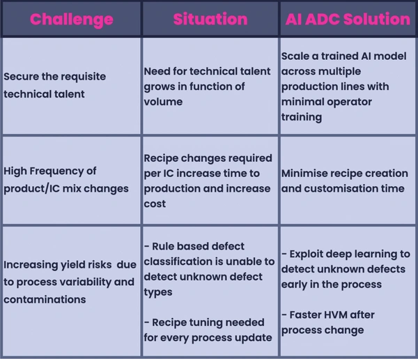
Cost-effective automated inspections are hard to achieve due to the shift towards high-mix low-volume production schemes. Development, introduction, and operation costs need to be justified in the context of changing production patterns.
When it comes to segments, automotive in particular, imposes great demands on defect inspection. A higher sampling rate for inspection is required, along with stricter screening criteria. Automotive applications often involve safety-critical components, making higher-quality chips even more crucial.
Overcoming these challenges requires a universal push for higher-quality chips across various device types and design nodes. Continuous improvements in inspection solutions that address complex IC architectures and adapt to changing production patterns are essential.
The Importance of Wafer Inspection
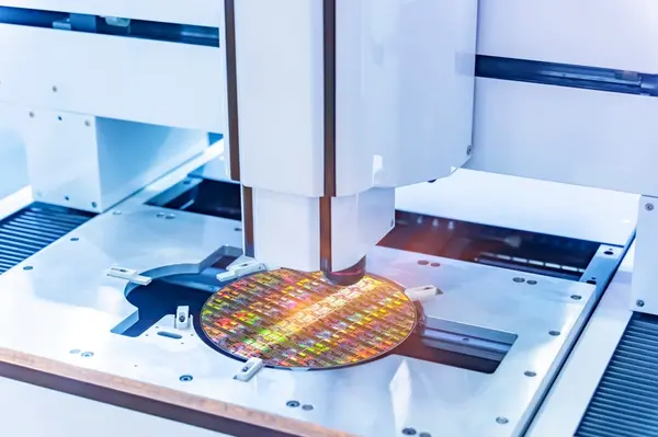
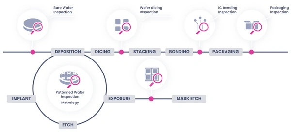
Semiconductor wafer production sites use inspection systems. These systems typically include tools for optical wafer inspection and scanning electron microscope (SEM)-based review for process monitoring. Both SEMs and optical inspection systems are used for defect detection in semiconductor wafer production. However, they differ in the type of defects they detect and the resolution of imaging capabilities.
Many production sites use a combination of both imaging tools. An optical microscope detects gross defects, while SEMs provide a more detailed view of these defects. SEMs also observe micro-defects invisible to optical microscopy. To design fabrication recipes and maintain process window parameters, chipmakers depend on wafer inspection, defect classification and review, metrology, and statistical analysis.
Semiconductor production involves multiple stages, from process technology development to yield ramp-up and high-volume manufacturing for a new node. At each stage, inline wafer inspection technology—especially wafer defect classification—plays a crucial role in improving and maintaining yield. Defect characterization allows chip manufacturers to identify the root cause of problems and take corrective action for faster ramp-up and time-to-market.
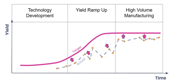
Yield Ramp-up and Comprehensive Process Control
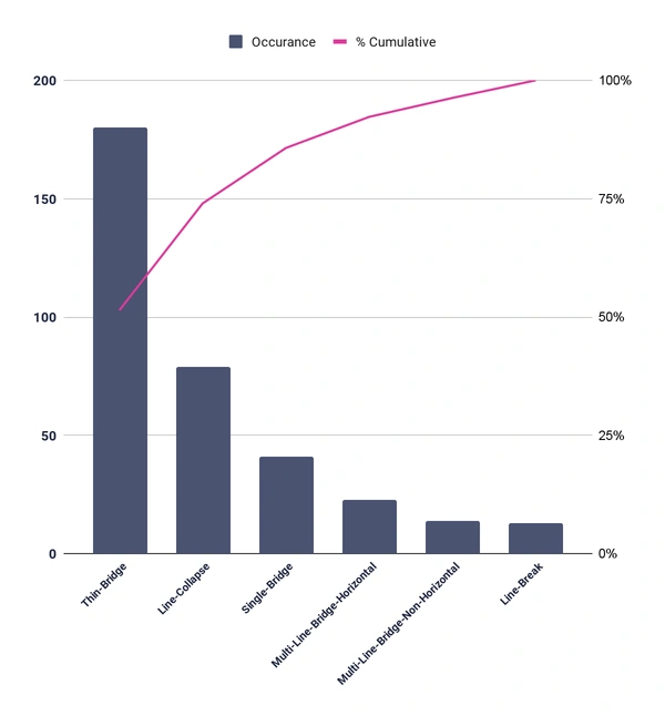
Defect classification is the act of allocating an image of a defect to a defect category. The goal is to decrease the number of defects that go unnoticed and predict maintenance needs in advance. It is important to have a highly accurate list of yield-limiting defects sorted by category, which is known as a fully classified Pareto. With this list, engineers quickly identify the specific types of defects causing the issue and discover the root cause more efficiently.
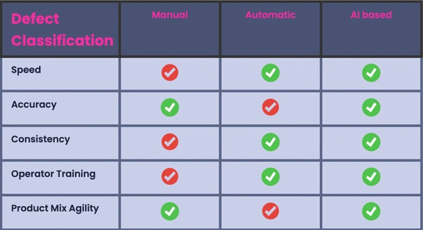
Manual defect classification is labor-intensive, repetitive, and requires highly trained employees. Results vary from operator to operator, and the end result is often less accurate than automated classification. Human visual limitation also means defects cannot be classified by people at scale.
Automatic Defect Classification (ADC) solutions mitigate the heavy load on human resources in fabrication. However, there remains an application mismatch between low classification accuracy and high purity needs. Deep Learning AI-based classifiers increase accuracy (intelligence) in defect classification for both existing and newly found defect types from an assortment of wafer designs.
AI-Based Automatic Defect Classification to the Rescue
Progressively Improving Accuracy
Technically, a Deep Learning AI model produces a set of confidence values for each class, then selects the highest confidence-scoring class as its prediction. During semiconductor manufacturing, classifications below the required confidence level (class threshold) for a specific class are labeled as “Unknown” and presented to the operator for manual classification.
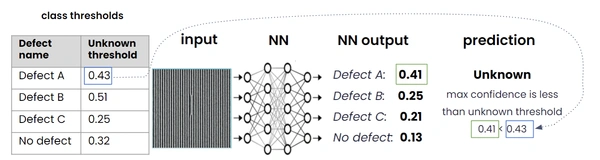
The manual classification augments the existing labeled data. It is then used to retrain the Machine Learning model—a way of working that avoids the time-consuming process of collecting new data for unseen defects.
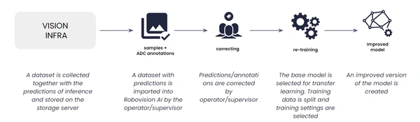
The confidence threshold per class can vary per IC fabrication layer, depending on actual factory performance. If defects are consistently found in a specific layer of the wafer, for example, the fab operator can modify the recipe. The confidence level increases, allowing for more images to be processed through manual classification. Overall confidence levels can also be improved in terms of available manual classification capacity. The result is a continuous refinement of the model, providing higher classification accuracy over a broader range of class types.
Tracking the real “Unknown Ratio” (percentage of classifications that do not reach the confidence level) versus the target “Unknown Ratio” serves as a trigger for model maintenance or vision infrastructure maintenance.
Minimize Operator Time on Recipe Creation
An ADC solution is no different from any other tool on the manufacturing floor. Just like an etcher or a polisher, ADC executes a recipe and produces a result. Additionally, as with any tool, the tool owner is responsible for creating new recipes and adjusting them from time to time as process changes are implemented.
Setting up an ADC is like training an operator. Just as a human trainee is subject to multiple examples of defects, ADC systems need a similar learning session. Also similar to evaluating a human trainee, the machine learning capabilities should be assessed and minor modifications made as necessary, based on the evaluation results.
The AI-ADC solution is built with an intuitive UI designed to guide users through the steps of collecting/managing samples, configuring image detection, setting up classifiers, and verifying results. The biggest difference is that only one ADC system needs training, rather than a small army of human reviewers.
One Size Fits All: AI Generalizes Over Different Layers And ICs
Defects in the complex chip manufacturing process are specific to the process layer and depend on the particular IC being fabricated. As such, recipes should either be capable of handling the variation or be customized to the specific layer or specific IC. Rule-based ADC struggles to generalize defects over ICs and process layers due to its nature. Consequently, it requires a consistent customization effort by highly skilled specialists.
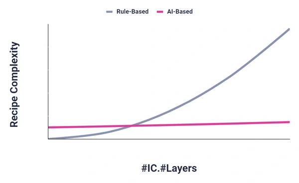
In chip manufacturing, different layers of interconnects in the Back End Of Line (BEOL) have distinct design rules that result in varying defect dimensions. However, the characteristics of the defects are comparable across the different layers. Consequently, AI-based recipes can be generalized across multiple layers and ICs, significantly increasing recipe creation and tuning efficiency.
Fabrication Challenges Solved by AI-ADC
Who Can Use AI-ADC?
The AI-ADC solution can be used in many different cases and industries where a machine captures a 2D or 3D signal and where defects can be classified by human inference. Theoretically, if operators can be trained to classify data, then it is reasonable to assume AI-ADC can be too. AI-ADC can also help identify otherwise overlooked defect types in a timely, consistent, and accurate manner.
A single AI-ADC solution accepts results from multiple defect scans and optical review systems in and across numerous manufacturing chains. With moderately powered hardware, it can process dozens of samples with multi-view images per second, compared to even the most skilled humans who can manage only one per second.
The high-speed, fast data acquisition handles a high volume of high-quality training data, and reliability allows the AI-ADC to be embedded inline. Most of the classifications can be done simultaneously or right after the inspection. Engineers identify problems early and act accordingly, translating to better yield and efficiency.
The enterprise-grade AI-ADC solution also fits multiple AI maturity levels. For organizations new to deep learning, the AI-ADC enables the creation of deep learning models. Users can train/test the model while avoiding the heterogeneous complexity of AI libraries. For organizations looking to prove models in production, the AI-ADC enables operators to integrate models and fit into production, offering optimized workflows and enhanced user experiences.
AI-Driven Wafer Inspection: The Future of Semiconductor Manufacturing
AI-driven wafer inspection is redefining semiconductor manufacturing, offering a scalable, high-precision solution to defect detection. By automating classification and optimizing quality control, AI minimizes human error, accelerates production, and boosts yield. As the industry evolves, integrating AI ensures manufacturers stay competitive, meeting the demands of complex chip architectures and high-performance standards. Investing in AI-powered inspection is not just an upgrade—it’s a strategic move toward greater efficiency, accuracy, and long-term success.
Discover how to boost accuracy, efficiency, and yield by transforming your wafer inspection with AI.