Inspection Beyond Rules: How Vision AI Accelerates Yield Ramp for OEMs
Date Section Blog
Semiconductor Yield Ramp: Why Quality Is Key
Production yield has the greatest impact on wafer processing outcomes. It drives output per unit of input resources, waste generation, time to market, and profitability. Although faster yield ramp means quicker breakeven and competitive edge, success depends on one factor above all else: quality.
Semiconductor manufacturers rely on rigorous inspection to reduce defects and improve yield quality. However, traditional and manual inspection methods fail to keep pace with process complexity. Subtle flaws go undetected, false alarms increase, and root-cause analysis slows, all of which impact yield and time-to-market for new products.
Vision AI changes the equation. Fabs equipped with this technology achieve wafer inspection at resolutions and speeds surpassing traditional optical rules. They can also handle ever-larger product mixes and support growing defect complexity. Yet, adoption remains fragmented. Many fabs lack an expert in the loop and deployments rarely scale. OEMs that embed vision AI into their inspection machinery close this gap, enabling fabs to achieve scalable deployment, faster yield ramp, and greater value from every tool.
This article explores how quality is the key driver for hitting yield, cost, and time-to-market targets. It discusses how vision AI-powered solutions address the limitations of traditional inspection, allowing quality inspection at scale. And how solutions like Robovision put domain experts directly in the AI loop through a low-code platform that augments inspection machinery with adaptive, continuously learning models.
Rising Defect Complexity in Semiconductor Manufacturing
A fast yield ramp promises competitive advantage that is critical in unpredictable economic environments. Production speed also allows new nodes to reach volume production earlier, securing premium pricing windows and customer trust.

Inspection machinery, however, must still deliver higher sensitivity and wider coverage. Tools must adapt across SKUs and nodes while keeping cost of ownership under control. In this context, quality is not optional but the driving force behind yield, cost, and product rollout time.
Escalating industry challenges add further pressure. The rise of 3D geometries (in transistors), new materials, and heterogeneous integration causes growing defect complexity. Short consumer product lifespans continually expand the range of required chip designs. While the evolution of chips under Moore’s Law, with transistor density doubling approximately every two years, demands ongoing advances in inspection equipment sensitivity. New chip functions driven by “More than Moore” innovation require enhanced production automation and quality control to cover growing volumes and handle the many possible failure modes of multi-technology devices (MEMS, photonics, etc). To meet demand and gain careful control of variability, manufacturers must increase coverage, speed, and throughput.
Enter rigorous inspection. Obviously, quality control measures using visual detection of (latent) defects or abnormalities ensure products meet strict industry standards. Likewise, these measures support long-term reliability of chips in applications like automotive, medical, and aerospace electronics. The automotive sector, for example, imposes high demand and defect inspection standards. It requires a higher sampling rate and has stricter screening criteria. Automotive applications also involve safety-critical components, driving the need for higher-quality chips.
But how do OEMS achieve both quality and speed? Especially as the development, introduction, and operation costs must be justified in the context of changing production patterns.

The Limitations of Traditional Inspection
These demands present challenges for traditional inspection solutions. Legacy approaches, including ML-based and rule-based solutions, are rigid and struggle with variability in defects. Tool-specific AOI systems lack adaptability across SKUs and process nodes. New defect types require extensive rule engineering, while cross-tool data remains siloed, delaying root cause analysis. When it comes to manual inspection, humans introduce variability and tire under repetitive conditions. Recognizing scratch and line types of defect patterns needs 100% focus, which is hard for human inspectors, especially when hidden defective dies may exist on the scratch contour and become discontinuity points. When large quantities of wafers are produced, human effort is even less effective. Yet manual inspection still accounts for 10–15% of visual quality checks (subject to differences in wafer types and fabs).
The result: inspections are fragmented and costly. Quality suffers, yield lags, and fabs face pressure from customers demanding better performance.
Driving Model Purity and Inspection Accuracy with AI-Powered Defect Classification
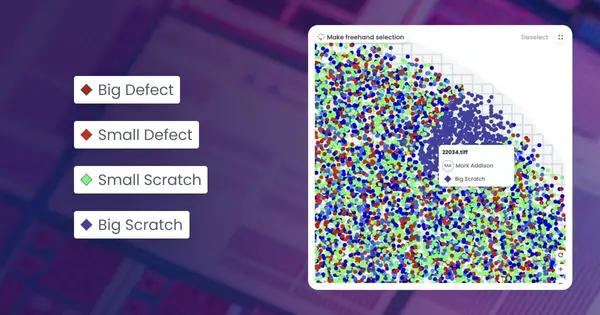
Vision AI has the potential to address these challenges. AI-powered automated defect classification (ADC) enables rapid and consistent inspection of semiconductor wafers. Whereas defect detection relies on high‑resolution wafer images, defect classification uses very small (512×512‑pixel) SEM micrographs taken at atomic scale, with defect positions sourced from the KRF file. Because each wafer yields numerous such micrographs, the system handles a large number of images per wafer. It recognizes minute irregularities far beyond human vision, reducing the risk of missing subtle flaws. The system also maintains uniform inspection criteria, avoiding variability that occurs with human inspectors or rigid rule-based algorithms.
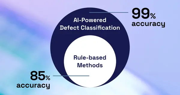
Systems with these capabilities potentially achieve detection rates up to 99%, compared with ~85% in rule-based methods. By minimizing recipe creation and customization time, AI ADC addresses the challenge of ever-changing product/IC mix. Domain expert reliance becomes less of a bottleneck, and models can be scaled across multiple production lines, tools, and sites.
Build Better Chips, See Better Yield
The Resource Bundle for Vision AI in Wafer Inspection

However, developing a robust AI-ADC model requires high-quality labeled images. Labeling is a challenging task that demands deep process engineering expertise, making human reviewers uniquely qualified and likely "trained" very well. That said, people make mistakes, have limited ability, and can only label effectively with context.
A centralized system, such as Robovision’s Purity Loop, overcomes this by streamlining data labeling and curation. The closed-loop feedback system is built to tackle complex and critical tasks, improving training data accuracy and pushing AI to act on its best behavior. Since the Robovision 5.10 AI platform deploys anywhere in a production environment, the Purity Loop continuously curates data at every stage to optimize model performance. Data selection is trained through tagging and filtering, so users can organize their data with metadata. The system allows users to easily inspect data through enhanced filtering and evaluate training data using graphical analysis of class distribution.
Continuous Learning and Process Optimization
Beyond scalability, AI ADC models bring another advantage: they continuously learn and optimize, improving accuracy and adaptability with every wafer inspected. Unlike static rule-based logic, AI models improve over time as they are exposed to new anomalies. These anomalies are then labelled by a domain expert, which triggers a new training cycle resulting in a new model. Stability and predictability are key: retraining is only done supervised by humans and approved before updating production models. The inspection models improve, feeding yield gains back into the process. Defect classification becomes more accurate and robust, and does not stagnate. Instead, it adapts to evolving conditions, gaining speed and precision.
For the fab, defect escape rates decrease over the tool lifecycle, and false alarm rates drop. One memory chip manufacturer showed a 15% drop in false positives within six months of continuous AI operation, purely from adaptive learning and the false calls it made.
Faster Yield Ramp
Yield ramp acceleration is another measurable benefit. TSMC reports 10–15% faster yield during the ramp-up of recent nodes through AI and machine learning. The most skilled humans can only manage around one sample per second. With vision AI, machines can process at a high inference-per-second rate and scale toward virtually unlimited throughput with improved hardware. Additionally, most classifications can be done at the same time or right after inspection, allowing engineers to identify problems early and act accordingly. Time and materials savings accrue with the ability to place lower-quality specimens into a different bin for use with less critical applications.
Predictive Maintenance and Downtime Reduction
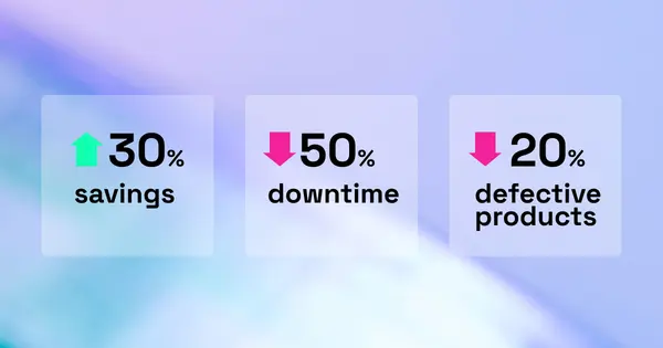
Predictive maintenance adds further gains. AI algorithms analyze data from equipment sensors to predict when maintenance is needed, saving fabs up to 30% compared to traditional solutions, and reducing unplanned downtime by up to 50%. Identifying potential quality issues reduces defective products by up to 20%, resulting in consistent production schedules and improved efficiency.
The OEM Opportunity: Defending Against Disruption
Customers no longer expect just machines; they seek solutions that improve their bottom line. This demand, together with the rise of vision AI, creates both challenges and opportunities. Incumbent machinery makers face pressure from digital-solution providers, aftermarket rivals, and rental operators offering flexible and customer-centric models. OEMs rooted in mechanical and optical engineering lack deep in-house digital expertise, resulting in complexity and risk when integrating hardware, software, and digital ecosystems. All compounded by an evolving landscape of new market players and technologies.
Robovision helps OEMs overcome barriers by embedding vision AI into machines in a scalable, customer-centric way. Its low-code platform and proven methodologies accelerate vision AI maturity, cutting time-to-market from proof of concept to full production. OEMs launch next-generation machines that combine physical and digital capabilities, deliver AI-enabled services across the equipment lifecycle, and participate in sustainable digital ecosystems. Just as importantly, Robovision provides a repeatable, organization-wide framework for developing AI products. The vision AI platform streamlines processes, lowers overhead, and reduces risk. OEMs stay agile and offer new value for customers, while defending against disruptive entrants. That value is supported by a steady release cycle: Robovision introduces new functionality every quarter, so the platform evolves year over year.
Turning Quality into Competitive Advantage
Robovision puts experts in the loop by equipping engineers to annotate wafer images, validate model outputs, and continuously refine AI performance. These capabilities liberate data scientists from lengthy development tasks, freeing them to drive innovation by experimenting and optimizing different algorithms for diverse use cases. A closed feedback cycle is created in which AI handles repetitive classifications while engineers concentrate on rare or critical defects, ensuring accuracy, trust, and adoption. By embedding domain expertise into the AI lifecycle, Robovision transforms vision AI from a black box into a trusted co-pilot for yield improvement.
With real-time, adaptive AI, Robovision delivers more than defect metrology and inspection. It provides proactive solutions that improve yield, optimize throughput, reduce cost, and strengthen market leadership. The platform enables domain experts to train, validate, and deploy scalable AI models across production lines with continuous learning and improvement. By adopting Robovision, OEMs reduce operational costs, cut time to market, and accelerate yield ramp: turning quality into a sustained strategic advantage.
Build Better Chips, See Better Yield
The Resource Bundle for Vision AI in Wafer Inspection