Enhance quality assurance, optimize automation, and improve safety
The Robovision AI platform gives you a fast track to smart solutions by integrating computer vision into your machinery. This helps you enhance quality assurance, optimize automation, and improve safety—all while embracing lean manufacturing principles.

Automated inspection
We help you automate the inspection process, so that every product meets the highest quality standards.

Defect Detection
Our platform excels at detecting even the most subtle defects. Fast and accurate. Day in, day out, 24/7.

Real-time Monitoring
Automated trend monitoring ensures timely maintenance and reduces unplanned downtime.
Improve your models with the Robovision AI Platform
Data Annotation
Label and annotate visual data with our powerful tools
Model Training
Upload large amounts of data to train new models
Model Optimization
Calculate the confidence you can have in your data and select the most useful samples to re-label
Accelerate Time to Reliable Operations
Robovision's platform drastically reduces the time required to deploy new AI solutions in your manufacturing environment.


Trusted Models with Continuous Improvement
Our platform ensures that your AI models are always performing at their best. With full traceability of data sources, consistent workflows that minimize human error, and robust model performance.


Cloud or On-Premises
No two manufacturing environments are the same, which is why Robovision’s platform offers flexible deployment options. Whether you need cloud-based solutions, on-premises setups, or a hybrid approach, our platform adapts to your specific needs.


Key Benefits of Robovision AI Platform in Manufacturing
Quality Assurance at Scale
100% of the products are automatically inspected at a speed and accuracy unmatched by human operators, ensuring consistent product quality across the board.
Enhanced Automation
Our platform can easily adapt to different product types, reducing setup and changeover times, and enabling production of a broad product assortment with minimal downtime.
Lean Manufacturing
By integrating AI into your manufacturing processes, you can identify and eliminate tasks with no added value, reduce inventory, and minimize waste.
Empower Operators
Computer Vision does more than just automate—it augments the abilities of your workforce, allowing operators to focus on higher-value tasks while optimizing quality and efficiency.
Success Stories

Robovision's AI platform was integrated into Niko’s injection molding process.
View success story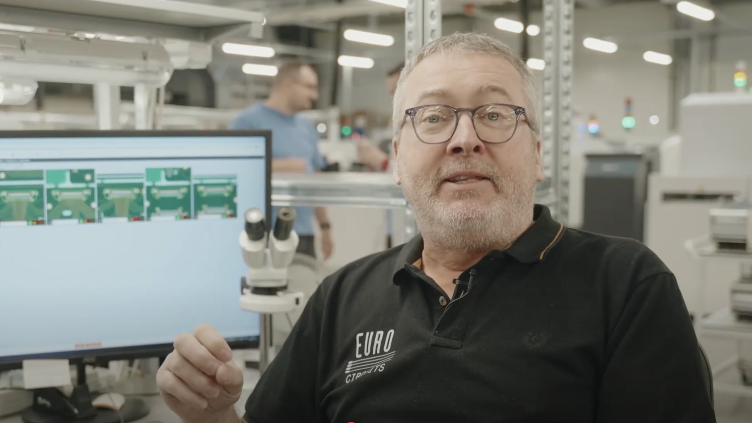
Robovision's AI Helps Eurocircuits Simplify and Perfect PCB Visual Inspection
View success story