Using AI for Wafer Inspection
Date Section Blog
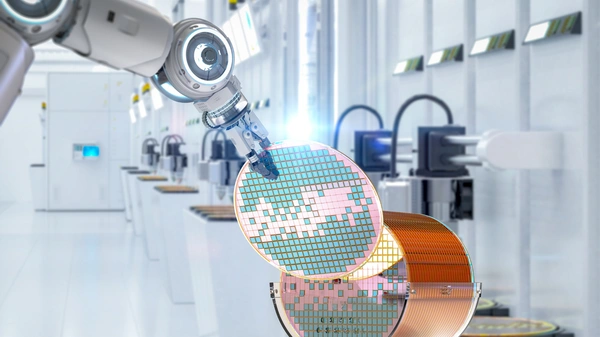
This is how Semiconductor players implement AI on the factory floor
As of 2022, it seems like AI is taking the world of quality control by storm. However, in the semiconductor industry, it seems like most players are only just starting to explore the possibilities of AI for chip inspection. Yet there is huge untapped potential in the combination of deep learning on the one hand and the latest visual sensors on the other hand. Nowadays, chip manufacturers can train defect detection and classification solutions to enable machines to hold out accurate wafer inspections. These automated processes of detection dramatically reduce dependence on manual efforts. For chip manufacturers, this increases consistency and expedites fabrication. Simply put: AI wafer inspection translates to higher yields and less waste.
Supervised versus unsupervised learning in semicon
Before we discuss the different approaches, it may be useful to clarify what can be fully automated (unsupervised learning) and what needs human intervention (supervised learning).
Pure defect detection can be realized using unsupervised techniques like anomaly detection. This type of algorithm can pinpoint irregularities that are imperceptible to humans in complex data in real time. As a consequence, the main benefit of using anomaly detection is the ability to find potential defects without knowing what they look like. By only showing non-defects examples, it learns what good samples look like and it can then find samples that deviate from the normal. However, when the algorithm detects anomalies, the user still needs to label them (or at least a subset of them) for automated classification.
Another unsupervised technique we can apply is Clustering. Clustering groups unlabelled examples according to similarity. Recommender engines, market and customer segmentation, and search results make extensive use of clustering. While this can be useful, a similarity cluster does not guarantee that different items in the cluster correspond to the same specific fault. However, these clustered patterns can be used for implementing supervised machine learning models. By labeling the cluster – and all samples within it – we can yield a training dataset for supervised learning models.
When it comes to implementing defect detection and identification solutions, we have identified 4 different approaches in the semicon space, each with its own advantages and challenges. In this blog post, we dive into these AI approaches for wafer visual inspection, exploring their pros and cons.
1. Deploying Full PreTrained Models
This approach involves the use of AI models that have been pre-trained on datasets of known defects. These models are designed to recognize specific fault mechanisms based on their training, making them ready for immediate deployment in the manufacturing process.
Pros:
- Quick Deployment
Full pretrained models can be deployed rapidly. This saves significant time and resources in model development and training. - High Accuracy for Known Defects
These models are highly effective at identifying known defects, which ensures reliable detection of common faults.
Cons:
- Limited Flexibility
The models are specialised for specific defects and might not adapt well to new or unseen fault mechanisms. This could lead to lower detection rates for novel defects. - Confusion
When having a process where only defects A and B are present, and another independent process where only A and C are involved, using a model that was pre-trained on A, B and C could lead to confusion when B and C are showing contradicting patterns. A model that was trained on specifically A and B and another model that was trained on A en C would yield potentially better results.
2. Offline Retraining by Solution Provider Support Team or by Internal AI Data Science Team
Off-line retraining allows for the customization of AI models based on new data collected from the manufacturing process. This method involves either the solution provider’s support team or an internal AI data science team retraining the model to recognize new or evolving defects.
Pros:
- Customization
Allows for retraining of the model to suit specific manufacturing environments and defect types, which allows for tailored solutions that can improve detection accuracy. - Continuous Improvement
As new defect data becomes available, you can retrain to recognise new patterns, which enhances the effectiveness of the models over time. You can allocate a fixed set of manual capacity to review and correct a low-confidence based selection of the inference results, which results in a constant upwards performance push of the model.
Cons:
- Time and Resource Intensive
Retraining models requires available human resources with the right domain expertise. These resources are typically scarce, which makes it hard to free them the moment you actually need the retraining. Especially with external parties involved, this process can take up to months. - Disruption to Production
The process of collecting data, retraining, and testing models offline may lead to delays in production if you need to take the inspection system offline for updates.
3. Retraining on the fab floor by Operator and Process Engineers
Online retraining empowers operators and process engineers to update the AI model in real-time, based on new defects and changes observed in the manufacturing process. This hands-on approach enables the model to adapt dynamically to the production environment.
Pros:
- Agile Model Development
During manufacturing you can train, evaluate/review and deploy models iteratively. Online retraining allows the model to adapt to new defects and changes in the manufacturing process in realtime. This results in a dynamic solution that evolves with the production line. - Empowerment of Staff
This approach engages operators and engineers directly in the AI process, leveraging their expertise to improve the model’s accuracy and relevance.
Cons:
- Risk of Overfitting
Without proper oversight, you risk to overfit a model to specific anomalies, which reduces its generalizability and effectiveness. - Training Complexity
Requires operators and engineers to have a certain level of expertise in AI and machine learning, which may necessitate additional training.
4. Using Digital Twins to Generate Datasets That Include Rare Defects
Digital twins simulate the manufacturing process and can generate datasets that include both common and rare defects. This approach provides AI models with a comprehensive training dataset, including defect scenarios that may not have occurred yet in the physical production line.
Pros:
- Comprehensive Training Data
Digital twins can simulate rare defects that might not be present in historical data, providing a more comprehensive dataset for training AI models. - Safe Testing Environment
This enables the testing and validation of AI models in a virtual environment without risking actual production, ensuring that the model is robust before deployment.
Cons:
- Complexity in Simulation
Creating accurate digital twins that faithfully represent the manufacturing process and potential defects can be complex and resource-intensive. - Possible Deviation from Reality
While digital twins are powerful tools, there might still be deviations between the simulated environment and real manufacturing conditions, potentially impacting the model’s accuracy when applied in practice.
In conclusion, each AI approach for wafer visual inspection offers a unique set of benefits and limitations. The choice of method depends on the specific requirements of the semiconductor manufacturing process, including the need for flexibility, the availability of resources, and the desired level of accuracy. Often, the best solution may be a combination of different approaches. It is not hard to imagine the advantages of using pre-trained models combined with online retraining.
By carefully considering these factors, manufacturers can select the most suitable AI strategy to enhance the quality and efficiency of wafer production.