Robovision 5.7: The Release Designed for the Semiconductor Industry
Date Section News
Semiconductor manufacturing is the invisible giant hand driving modern life. Every device—be it a smartphone, computer, robotic vacuum cleaner or car—functions thanks to a tiny chip inside. Delicate and intricate, these chips are increasingly difficult to perfect. In a world where a microscopic defect can derail an entire production line, the challenge for semiconductor manufacturers is immense: how do you increase yield without compromising quality?

This is the age-old struggle of semiconductor fabs. For decades, the industry relied on meticulous manual inspection, rule-based defect detection systems, and human operators to catch these errors. Yet, as chips become smaller and their architectures more complex, traditional methods are reaching their limits. The industry needs smarter, faster, more adaptable solutions that can keep pace with technology's relentless progress.
Enter Robovision 5.7, the AI-powered vision platform that promises to reshape the landscape of semiconductor manufacturing. Powered by deep learning, this platform is more than just another inspection tool—it’s a giant leap forward, designed to tackle the challenges of tomorrow’s fabs with unparalleled accuracy and adaptability.
But what makes Robovision 5.7 so revolutionary? How semiconductor manufacturers everywhere will experience the game changing platform is explained below.
The Defect Dilemma
A semiconductor wafer is essentially a silicon canvas, on which microscopic circuits are etched. This process, known as lithography, happens with pinpoint precision, layer by layer, until the final product—an integrated circuit—is ready for assembly. The tiniest imperfection in this process, however, can render an entire chip defective. And when you’re producing wafers with hundreds or thousands of chips, that risk multiplies exponentially.
Traditionally, fabs have relied on rule-based systems to identify defects. These systems follow pre-programmed rules to detect anomalies in the manufacturing process. While they’ve served the industry well for years, their limitations are becoming increasingly apparent as chip designs become more intricate and defect profiles more diverse.
Imagine trying to find a needle in a haystack while the haystack is shrinking, and the needle is constantly changing shape. That’s the dilemma semiconductor fabs face with traditional defect detection methods.
Imagine trying to find a needle in a haystack while the haystack is shrinking, and the needle is constantly changing shape. That’s the dilemma semiconductor fabs face when using traditional defect detection methods. They simply can’t keep up with the ever-evolving nature of defects or the increasing complexity of modern chip designs.
This is where Robovision 5.7 comes in. Powered by deep learning AI, it doesn’t rely on static rules—it learns, adapts, and evolves. The more defects it encounters, the better it gets at spotting them. And it doesn’t just stop at identifying defects; it classifies them with a precision that far surpasses human capabilities.
The Birth of Robovision’s Automatic Defect Classification
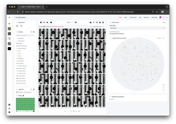
With KRF file support, Robovision 5.7 transforms wafer maps into interactive tools that allow engineers to visualize defects, pinpoint their locations, and take corrective action with ease. This release also introduces the Split View. This interface allows users to view wafer maps and defect images side-by-side, streamlining the inspection process and making it easier to identify and classify defects. No more toggling between screens or sifting through endless data—everything is presented clearly and intuitively, allowing engineers to focus on what matters most: improving yield.
The Power of Continuous Improvement: The Purity Loop

In any AI-based system, the quality of the training data is critical to the accuracy of the model. But here’s the catch—human-labeled data is inherently prone to error. Even the most skilled operators can make mistakes, which can limit the AI model's accuracy.
So, how to achieve the near-perfect accuracy required in semiconductor manufacturing? Enter Robovision’s Purity Loop.
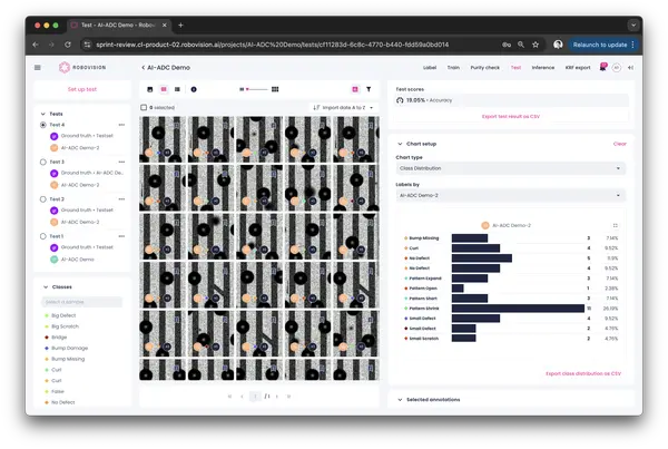
The Purity Loop is a continuous improvement cycle that allows the AI model to assess the quality of its own training data and correct inconsistencies. The system compares its own classifications with the human-assigned labels and identifies discrepancies. These discrepancies are then visualized in a Confusion Matrix, which highlights differences between human and machine labeling.
Poorly labeled data can be flagged and sent back to the Label Center for reevaluation, creating a feedback loop that continuously improves the accuracy of the model. Over time, the model becomes more accurate, achieving the high level of precision required for semiconductor defect classification.
This iterative process is what sets Robovision 5.7 apart from other AI platforms: this loop allows you to trust your data.
Adapting to the Evolving Nature of Defects
One of the biggest challenges in semiconductor manufacturing is the ever-evolving nature of defects. As device architectures become more complex and new materials are introduced, the types of defects that occur change as well. Traditional rule-based systems struggle to keep up with these changes, as they are designed to detect specific types of defects based on predefined criteria.
Robovision 5.7, however, thrives in this environment. Its deep learning algorithms are not bound by static rules—they continuously learn and adapt to new defect profiles as they emerge. This makes it an ideal solution for fabs that are working with cutting-edge technologies and need to stay ahead of the curve.
For example, as 3D geometries become more common in semiconductor manufacturing, new types of defects are emerging that are difficult to detect with traditional methods. Robovision’s ADC is uniquely equipped to handle these challenges, as it can analyze complex 3D structures and identify subtle defects that might go unnoticed by other systems.
This adaptability is critical for fabs that are constantly pushing the boundaries of what’s possible in chip design and manufacturing. With Robovision 5.7, they can rest assured that their defect classification system will keep pace with the rapid evolution of the industry.
The Efficiency Revolution: Faster Inspections, Higher Yields
In the fast-paced world of semiconductor manufacturing, every second a wafer spends on the production line is a second that could impact yield and profitability. Traditional inspection methods are time-consuming and labor-intensive, requiring skilled operators to manually review thousands of images and identify defects.
Robovision 5.7 changes all that. Its AI-powered ADC dramatically reduces inspection times by analyzing images in real-time and identifying defects with unmatched precision and consistency. Not only does this speed the inspection process but also reduces the likelihood of human error, resulting in higher yields and lower costs.
But it’s not just about speed—Robovision 5.7 also helps fabs optimize their workflows by automating the defect classification process. Instead of relying on manual inspections, fabs can now use AI to classify defects automatically, freeing up operators to focus on more critical tasks.
Scalability: Expanding Across Multiple Facilities and Production Lines

As semiconductor manufacturers grow and expand operations, the need for scalable solutions increases in importance. A solution that works well in one fab may not necessarily work in another, especially when different product types and defect profiles are involved.
Robovision 5.7 addresses this challenge by offering a scalable platform that can easily adapt to different production environments. Whether you’re working with a single fab or managing multiple facilities, Robovision’s AI platform can be customized to meet specific needs.
The platform’s API integration allows fabs to seamlessly incorporate Robovision 5.7 into their existing workflows, ensuring a smooth transition and minimal disruption to production. And with the ability to support a wide range of hardware devices, Robovision 5.7 is the perfect fit for fabs looking to optimize their operations across multiple production lines.
The Future of Semiconductor Manufacturing
The semiconductor industry is in the midst of a revolution. As chips become smaller, faster, and more powerful, the need for advanced defect classification systems has never been greater. Traditional methods are no longer enough to keep pace with the rapid evolution of chip design and manufacturing processes.
We worked hard to make Robovision 5.7 a future-proof solution for semiconductor defect classification. Its deep learning algorithms, continuous improvement cycles, and adaptable platform make it the ideal solution for fabs looking to stay ahead of the curve. With Robovision 5.7, fabs can improve yield, reduce costs, and optimize their workflows—all while embracing the cutting-edge technologies that are driving the next generation of semiconductor innovation.
In this silent revolution, where the stakes are microscopic but the impact is monumental, Robovision 5.7 is ready to be challenged. It’s not just about finding defects—it’s about transforming the entire manufacturing process, bringing clarity to the chaos and turning complexity into opportunity.